
วันอังคารที่ 28 สิงหาคม พ.ศ. 2555
วันศุกร์ที่ 24 สิงหาคม พ.ศ. 2555
PCB
PCB (Printed Circuit Board)
1.) Classify by Rigid or Flex
1.1) Rigid PCB
Most PCB is rigid PCB that use with the general application from normal / base electronic equipment/device until aerospace, avionics, military, medical device


1.2) FPC (Flexible Printed Circuit Board)
FPC is use for the application device which need to be bend or curve area and also a small area such as Printer pare wires , digital camera, game, hard disk drive, mobile phone, car gauge meter console.


1.3) Rigid + Flex PCB
Use bothe Rigid and Flex PCB in the same PCB which depend on user design.


2.) Classify by Complexity of PCB layer
2.1) Single Side PCB
Single-Side PCB is the simplest and most common type of PCB. It was the first device used for the interconnection and assembly of electronic components forming a cohesive and functional operating system. The primary industry that uses these boards is the consumer electronics industry.
2.2) Double Side PCB
Double Side PCB have made circuit in 2 layer of different PCB side that both layer has connect by via PTH (Plated Through Hole) which depend on design this is more complex than Single Side PCB.

2.3) Multi Layer PCB
Multi Layer PCB have more layer than double side PCB, it has many circuit layer between Top side and Bottom side of PCB and also each layer can connect with via PTH (Plated Through Hole), this type is more complex than double side PCB.

2.4) High Density Interconnect (HDI) PCBs
HDIs have a higher circuit density per unit area than the conventional multi-layered PCBs. They also have a smaller hole diameter, a higher line density and a greater connecting density with more connecting points per square inch than that employed in conventional PCB technology. HDIs are used to reduce size and weight, as well as to enhance the electrical performance of electronic products such as those found in smartphones nowadays.
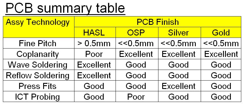
3.) Classify by Surface Finish
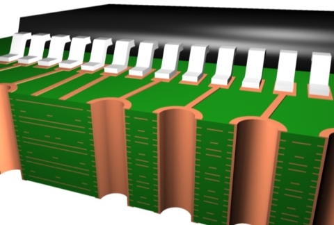
3.1) Hot air solder levelling (HASL)
HASL is the cheapest surface finished which is the method of diping the PCB into the molten solder bath so he copper surfaces are covered by solder.

Brief Process Flow of HASL
Step 1 : Pre-Clean ==> Done with micro-etch
Step 2 : Fluxing ==> To protect oxidation, Affect heat transfer during solder immersion.
Step 3 : Hot Air Leveling ==> For SnPb Molten solder temperature 460 F (237 C), For Lead-Free not yet have information.
Step 4 : Post-Clean
Typical Thickness : 25 - 2,000 Micro inches (mils)
Advantages of HASL
- Excellent wetting during component soldering
- Easily applied
- Easily Rework component
- Good bond / joint strength after PCBA
- Long Shelf Life
- Easy to visual inspection
Disadvantages of HASL
- Low planarity makes this surface finish unsuitable for use with fine pitch components, high risk to have solder paste printing and assembly defect.
- High thermal stress during process may introduce defects to PCB.
- High risk to generate solder bridging on fine pitch component.
- Inconsistence coating thickness (on vary pad size).
3.2) Organic Solder Preservative (OSP)
OSP is the coating the thin organic on copper surface that was simple and easy way to do and the thin OSP coated will limited the number of passing heat cycle 2 - 3 times maximum because the organics coated will be disappear about 25 % every times pass heating (especially reflow process)

Typical Thickness : 8 - 24 Micro inches (mils), 0.2 - 0.6 microns
Advantages of OSP
- Flat, Coplanar pad
- Reworkable
- Low cost
- Short and easy process
- Good solder mask intergrity
Disadvantages of OSP
- The thin coating is effect to reliability when pass many time of heat
- Sensitive to some solvent, if need clean after mis-print need to check solvent, some solvent may effect the coating removed that leading to exposed copper problem.
- Limited shelf Life
3.3) Electroless-Nickel Immersion Gold (ENIG)
Plate Nickel on copper then plate Gold on Nickel

Typical Thickness :
==> Nickel 125 - 250 Micro inches (mils)
==> Gold 3 - 8 Micro inches (mils)
Advantages of ENIG
- Long Shelf Life
- Excellent flat planarity, consistence thickness
- Withstands multiple reflows
- Good Solderability
- Good for fine pitch component.
Disdvantages of ENIG
- The electroless nickel layer is brittle and has been found to break up during mechanical stress. This effect is known in the industry as 'black pad' or 'mudflat cracking'. This has lead to bad press for ENIG
- Higher cost (5X HASL)
- Not wire-bondable
- Too high Gold thickness generate de-wetting problem when soldering because too high thickness of gold is hard to absorb heat.
- Can not rework surface finished (ENIG) at PCB fabricator.
3.4) Immersion Silver (Ag)
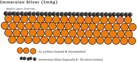
Typical Thickness :
==> 5 - 25 Micro inches (mils)
Advantages of Immersion Silver
- Good for fine pitch component
- Planar Surface
- Inexpensive
- Short, easy process cycle
- Long shelf life
- Can be reworked the silver surface at PCB fabricator
- Compatible for Lead-Free process.
- Surface suitable for electrical contact
- Capable of multiple reflow cycles
Disdvantages of Immersion Silver
- Tarnish must be controlled
- Rapid degradation of surface due to oxidation or contamination (with e.g. sulfur or chlorine)
- Not good for sliding connectors
- Occasional voiding
- Deposit gradually discolors due to air exposure
3.5) Immersion Tin (Sn)
Typical Thickness :
==> 25 - 60 Micro inches (mils)
Advantages of Immersion Tin (Sn)
- Good for fine pitch component
- Planar Surface
- Inexpensive
- Good solderability / hole filling ? ?
- Suitable for press-fit applications because no burr appears
Disdvantages of Immersion Tin (Sn)
- Limited rework cycles
- Sensitive on scratches
- Sensitive on thermal influence and improper storage conditions
===================================
Reference
http://www.kingboard.com/Item/list.asp?id=1234http://easypcb.xonelectronics.com/surface_finish_options.htm
http://en.wikipedia.org/wiki/HASL
http://www.saturnelectronics.com/technology_hub/immersion_silver_finish.html
วันพฤหัสบดีที่ 16 สิงหาคม พ.ศ. 2555
SMD and Component Package
SMD is " Surface Mount Device " it is the SMT electronic components which mount by surface mounting machine or placement machine , for the example as Resistor, Capacitor, Diode, Transistor, BGA, IC each package (SOP, SOIC, SOT, PLCC, etc .. )
Two-terminal packages
- Chip Resistor and Chip Capacitor
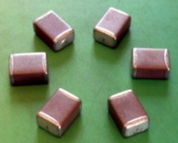


Rectangular passive components (mostly resistors and capacitors):
01005 (0402 metric): 0.4 x 0.2 mm (0.016 x 0.0079 in)
0201 (0603 metric): 0.6 x 0.3 mm (0.024 x 0.012 in)
0402 (1005 metric): 1.0 x 0.5 mm (0.039 x 0.020 in)
0603 (1608 metric): 1.6 x 0.8 mm (0.063 x 0.031 in)
0805 (2012 metric): 2.0 x 1.25 mm (0.079 x 0.049 in)
1008 (2520 metric): 2.5 x 2.0 mm (0.098 x 0.079 in)
1206 (3216 metric): 3.2 x 1.6 mm (0.13 x 0.063 in)
1210 (3225 metric): 3.2 x 2.5 mm (0.13 x 0.098 in)
1806 (4516 metric): 4.5 x 1.6 mm (0.18 x 0.063 in)
1812 (4532 metric): 4.5 x 3.2 mm (0.18 x 0.13 in)
2010 (5025 metric): 5.0 x 2.5 mm (0.20 x 0.098 in)
2512 (6432 metric): 6.4 x 3.2 mm (0.25 x 0.13 in)
2920: 7.4 x 5.1 mm (0.29 x 0.20 in)
- Tantalum capacitors length (typ.) x width (typ.) x height (max.)
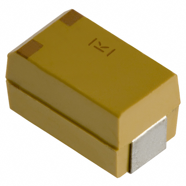
EIA 2012-12 (Kemet R, AVX R): 2.0 mm x 1.3 mm x 1.2 mm
EIA 3216-10 (Kemet I, AVX K): 3.2 mm x 1.6 mm x 1.0 mm
EIA 3216-12 (Kemet S, AVX S): 3.2 mm x 1.6 mm x 1.2 mm
EIA 3216-18 (Kemet A, AVX A): 3.2 mm x 1.6 mm x 1.8 mm
EIA 3528-12 (Kemet T, AVX T): 3.5 mm x 2.8 mm x 1.2 mm
EIA 3528-21 (Kemet B, AVX B): 3.5 mm x 2.8 mm x 2.1 mm
EIA 6032-15 (Kemet U, AVX W): 6.0 mm x 3.2 mm x 1.5 mm
EIA 6032-28 (Kemet C, AVX C): 6.0 mm x 3.2 mm x 2.8 mm
EIA 7260-38 (Kemet E, AVX V): 7.3 mm x 6.0 mm x 3.8 mm
EIA 7343-20 (Kemet V, AVX Y): 7.3 mm x 4.3 mm x 2.0 mm
EIA 7343-31 (Kemet D, AVX D): 7.3 mm x 4.3 mm x 3.1 mm
EIA 7343-43 (Kemet X, AVX E): 7.3 mm x 4.3 mm x 4.3 mm
- Aluminum capacitors
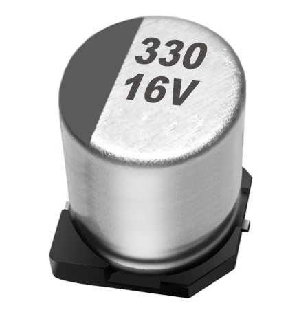
(Panasonic / CDE A, Chemi-Con B): 3.3 mm x 3.3 mm
(Panasonic B, Chemi-Con D): 4.3 mm x 4.3 mm
(Panasonic C, Chemi-Con E): 5.3 mm x 5.3 mm
(Panasonic D, Chemi-Con F): 6.6 mm x 6.6 mm
(Panasonic E/F, Chemi-Con H): 8.3 mm x 8.3 mm
(Panasonic G, Chemi-Con J): 10.3 mm x 10.3 mm
(Chemi-Con K): 13.0 mm x 13.0 mm
(Panasonic H): 13.5 mm x 13.5 mm
(Panasonic J, Chemi-Con L): 17.0 mm x 17.0 mm
(Panasonic K, Chemi-Con M): 19.0 mm x 19.0 mm
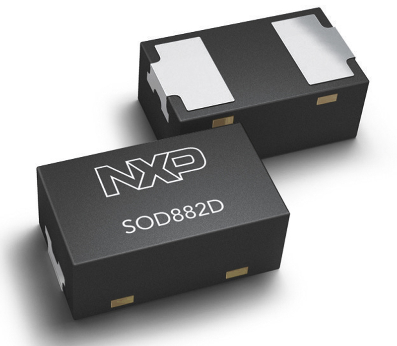
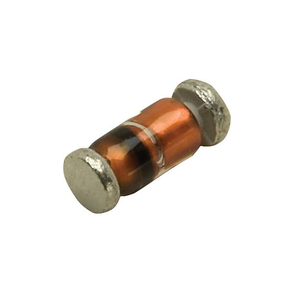
- SOD: Small Outline Diode

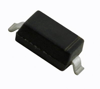

SOD-723: 1.4 x 0.6 x 0.59 mm
SOD-523: 1.25 x 0.85 x 0.65 mm
SOD-323 (SC-90): 1.7 x 1.25 x 0.95 mm
SOD-128: 5 x 2.7 x 1.1 mm
SOD-123: 3.68 x 1.17 x 1.60 mm
SOD-80C: 3.50 x 1.50 x ....
- MELF (Metal Electrode Leadless Face): mostly resistors and diodes; barrel shaped components, dimensions do not match those of rectangular references for identical codes.
MicroMelf (MMU) Size 0102: length: 2.2 mm, diam.: 1.1 mm.
MiniMelf (MMA) Size 0204: length: 3.6 mm, diam.: :1.4 mm.
Melf (MMB) Size 0207: length: 5.8 mm, diam.: 2.2 mm.
Three and Four terminal packages
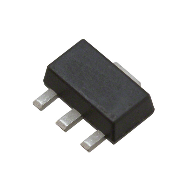
- SOT: Small Outline Transistor, three terminals
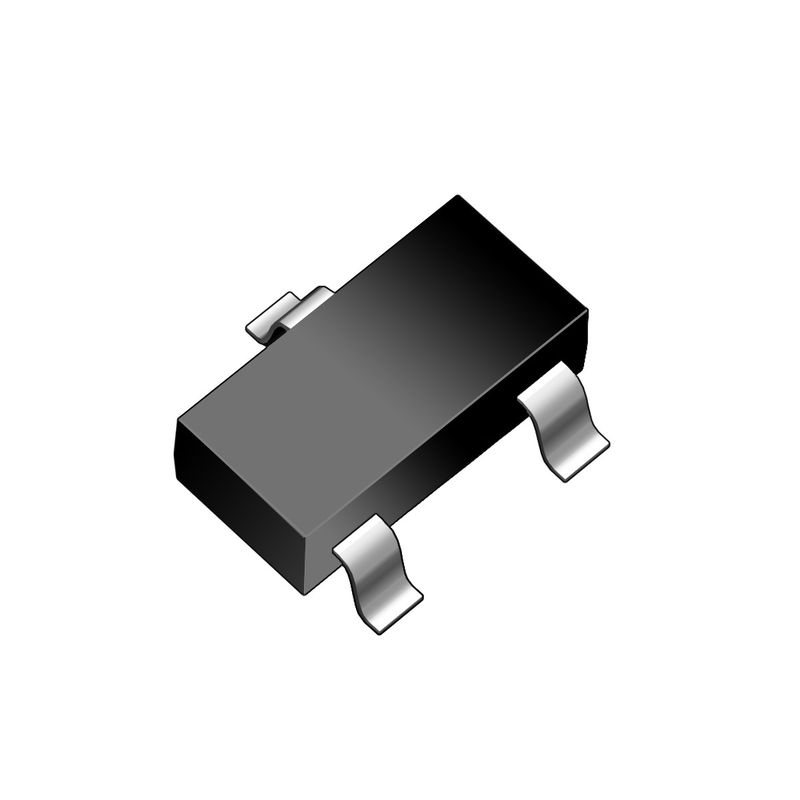
- SOT-23 (SC-59, TO-236-3): 2.9 mm x 1.3/1.75 mm x 1.3 mm body: three terminals for a transistor
- SOT-323 (SC-70): 2 mm x 1.25 mm x 0.95 mm body: three terminals
- SOT-416 (SC-75): 1.6 mm x 0.8 mm x 0.8 mm body: three terminals
- SOT-663: 1.6 mm x 1.6 mm x 0.55 mm body: three terminals
- SOT-723: 1.2 mm x 0.8 mm x 0.5 mm body: three terminals: flat lead
- SOT-883 (SC-101): 1 mm x 0.6 mm x 0.5 mm body: three terminals: leadless
- SOT-223: 6.7 mm x 3.7 mm x 1.8 mm body: four terminals, one of which is a large heat-transfer pad

- SOT-89: 4.5 mm x 2.5 mm x 1.5 mm body: four terminals, center pin is connected to a large heat-transfer pad
- DPAK (TO-252): Discrete Packaging. Developed by Motorola to house higher powered devices. Comes in three- or five-terminal versions

- D2PAK (TO-263): bigger than the DPAK; basically a surface mount equivalent of the TO220 through-hole package. Comes in 3, 5, 6, 7, 8 or 9-terminal versions
- D3PAK (TO-268): even larger than D2PAK
Five and six terminal packages
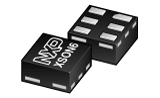
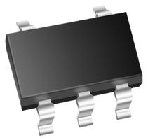
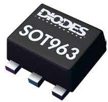
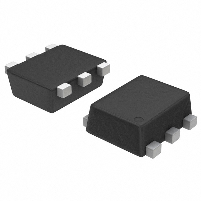
SOT: small-outline transistor, with Five and six terminal packages
- SOT-23-5 (SOT-25): 2.9 mm x 1.3/1.75 mm x 1.3 mm body: five terminals
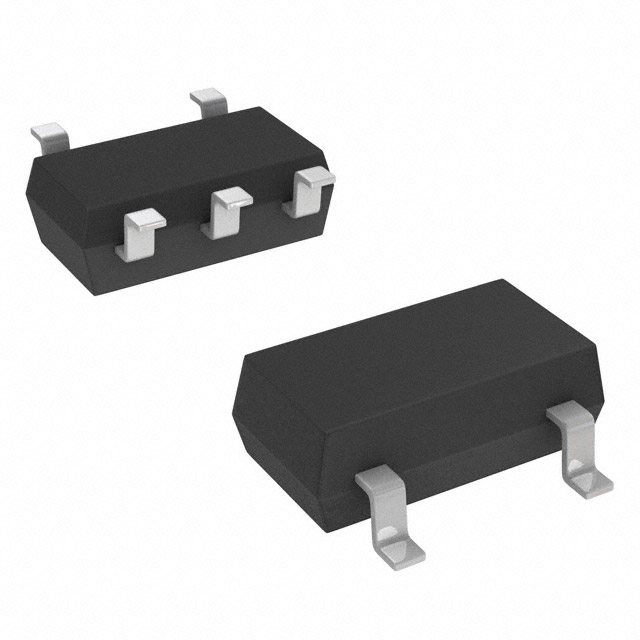
- SOT-23-6 (SOT-26): 2.9 mm x 1.3/1.75 mm x 1.3 mm body: six terminals

- SOT-23-8 (SOT-28): 2.9 mm x 1.3/1.75 mm x 1.3 mm body: eight terminals

- SOT-353 (SC-88A): 2 mm x 1.25 mm x 0.95 mm body: five terminals
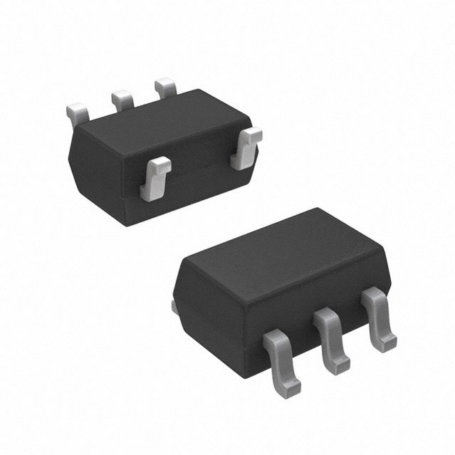
- SOT-363 (SC-88, SC-70-6): 2 mm x 1.25 mm x 0.95 mm body: six terminals

- SOT-563: 1.6 mm x 1.2 mm x 0.6 mm body: six terminals

- SOT-665: 1.6 mm x 1.6 mm x 0.55 mm body: five terminals

- SOT-666: 1.6 mm x 1.6 mm x 0.55 mm body: six terminals

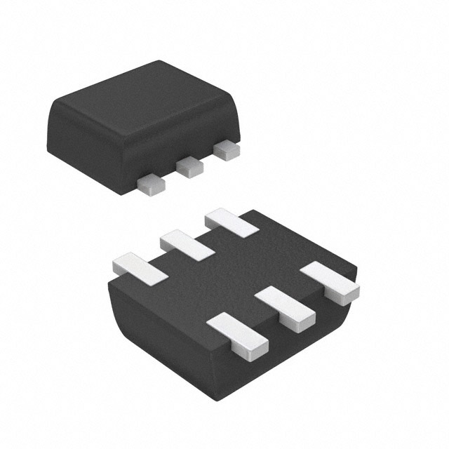
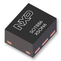
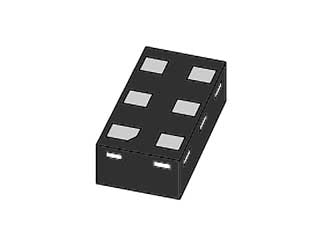
- SOT-886: 1.5 mm x 1.05 mm x 0.5 mm body: six terminals: leadless

- SOT-891: 1.05 mm x 1.05 mm x 0.5 mm body: six terminals: leadless
- SOT-953: 1 mm x 1 mm x 0.5 mm body: five terminals

- SOT-963: 1 mm x 1 mm x 0.5 mm body: six terminals
Dual-in-line
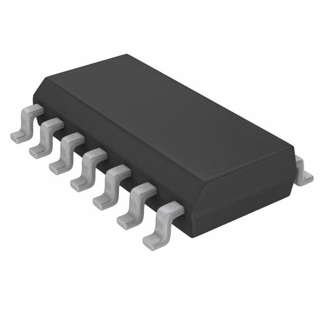
- SOIC: (Small-Outline Integrated Circuit), dual-in-line, 8 or more pins, gull-wing lead form, pin spacing 1.27 mm
Pictures : SOIC_001, SOIC_002


- TSOP: Thin Small-Outline Package, thinner than SOIC with smaller pin spacing of 0.5 mm


- SSOP: Shrink Small-Outline Package, pin spacing of 0.65 mm, sometimes 0.635 mm or in some cases 0.8 mm


- TSSOP: Thin Shrink Small-Outline package.

- QSOP: Quarter-Size Small-Outline package, with pin spacing of 0.635 mm

- VSOP: Very Small Outline Package, even smaller than QSOP; 0.4, 0.5 mm or 0.65 mm pin spacing

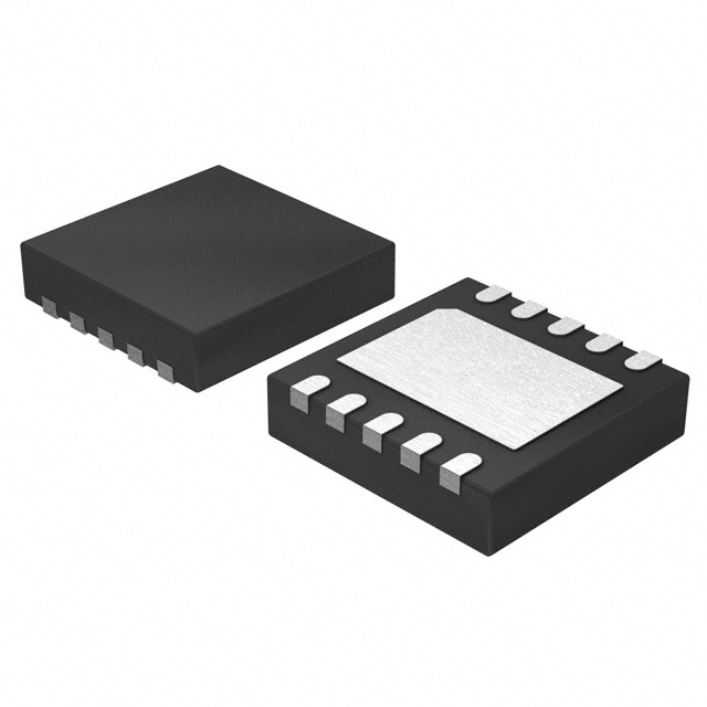
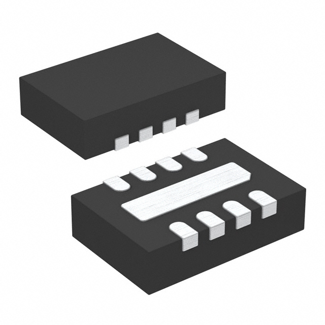
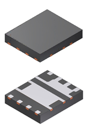
- DFN: Dual Flat No-lead, smaller footprint than leaded equivalent
Quad-in-line
- PLCC: Plastic Leaded Chip Carrier, square, J-lead, pin spacing 1.27 mm

- QFP: Quad Flat Package, various sizes, with pins on all four sides

- LQFP: Low-profile Quad Flat Package, 1.4 mm high, varying sized and pins on all four sides
- PQFP: Plastic Quad Flat-Pack, a square with pins on all four sides, 44 or more pins
- CQFP: Ceramic Quad Flat-Pack, similar to PQFP
- MQFP: Metric Quad Flat Pack, a QFP package with metric pin distribution
- TQFP: Thin Quad Flat Pack, a thinner version of PQFP
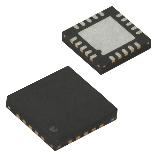
- QFN: Quad Flat No-lead, smaller footprint than leaded equivalent

- LCC: Leadless Chip Carrier, contacts are recessed vertically to "wick-in" solder. Common in aviation electronics because of robustness to mechanical vibration.


- MLP (MLF): Micro Leadframe Package (Micro Lead-Frame package) with a 0.5 mm contact pitch, no leads (same as QFN)
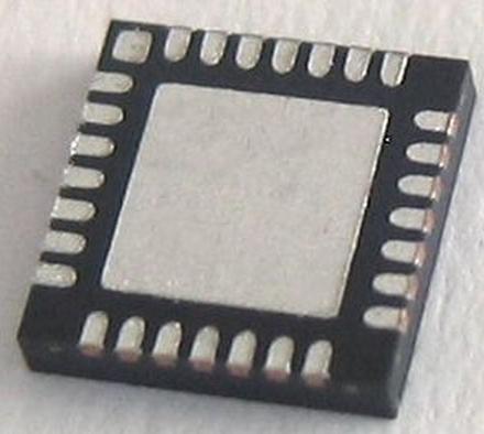
- PQFN: Power Quad Flat No-lead, with exposed die-pad[s] for heatsinking


Grid arrays
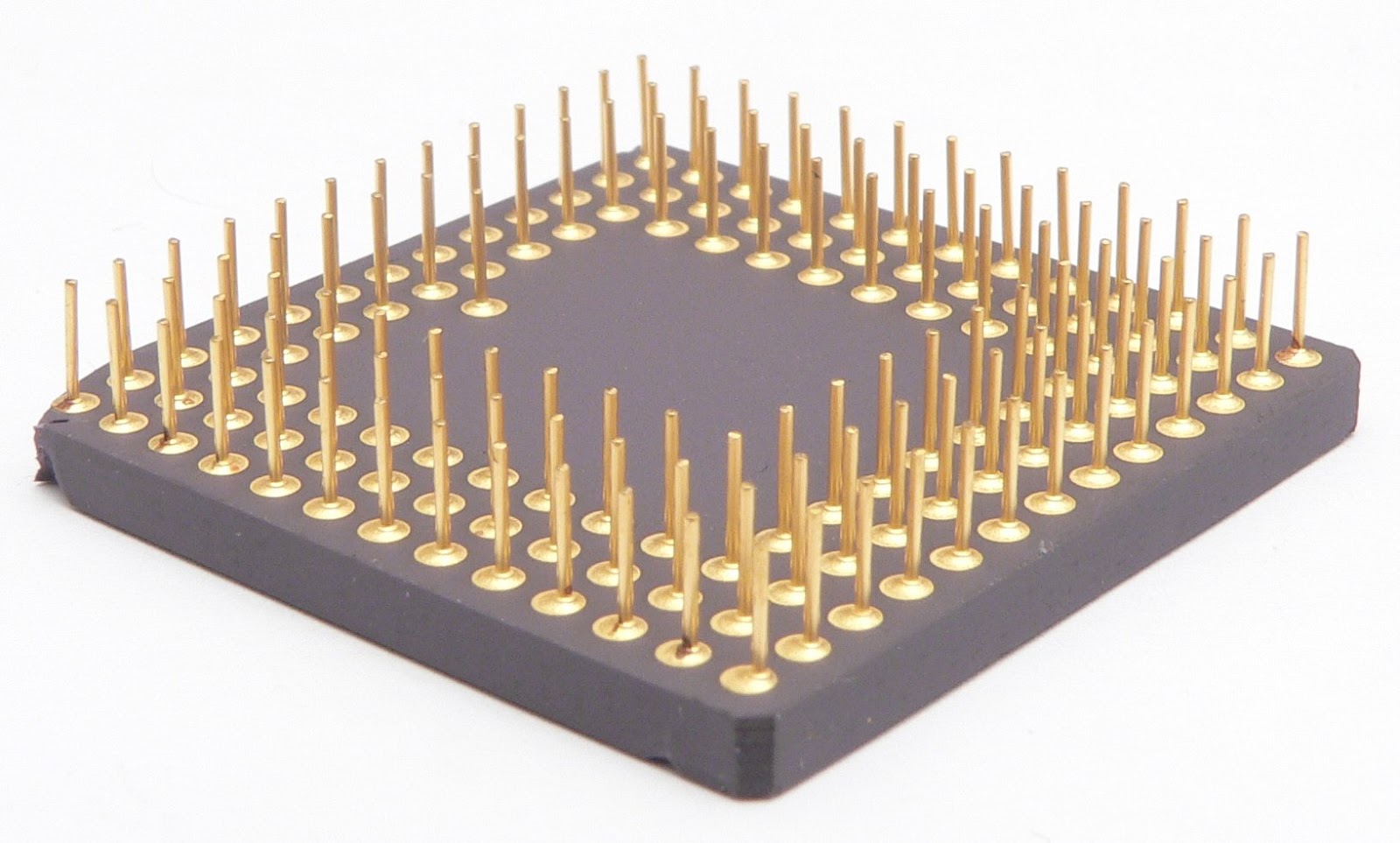
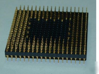
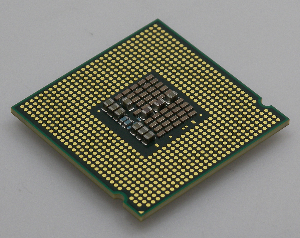
- PGA: Pin grid array.
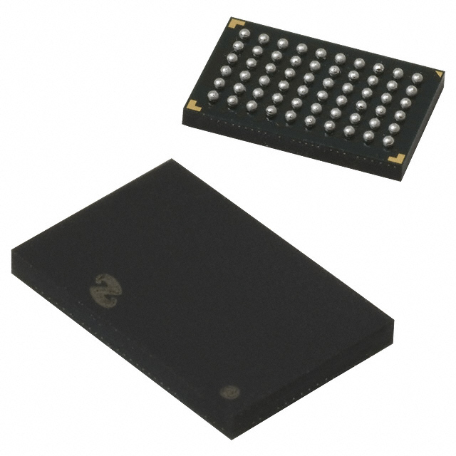
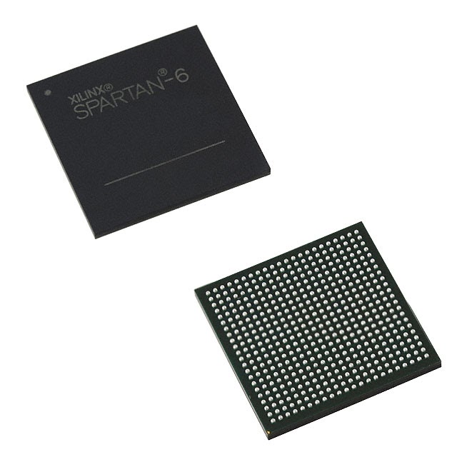
- BGA: Ball Grid Array, with a square or rectangular array of solder balls on one surface, ball spacing typically 1.27 mm


- LGA: An array of bare lands only. Similar to in appearance to QFN, but mating is by spring pins within a socket rather than solder.

- FBGA: Fine pitch Ball Grid Array, with a square or rectangular array of solder balls on one surface
- LFBGA: Low profile Fine pitch Ball Grid Array, with a square or rectangular array of solder balls on one surface, ball spacing typically 0.8 mm
- TFBGA: Thin Fine pitch Ball Grid Array, with a square or rectangular array of solder balls on one surface, ball spacing typically 0.5 mm
- CGA: Column Grid Array, circuit package in which the input and output points are high temperature solder cylinders or columns arranged in a grid pattern.
- CCGA: Ceramic Column Grid Array, circuit package in which the input and output points are high temperature solder cylinders or columns arranged in a grid pattern. The body of the component is ceramic.
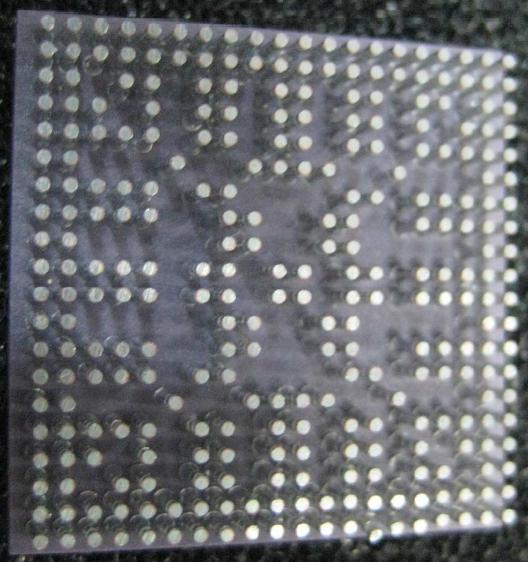

- BGA: micro-BGA, with ball spacing less than 1 mm
- LLP: Lead Less Package, a package with metric pin distribution (0.5 mm pitch).
Non-packaged devices (although surface-mount, these devices require specific process for assembly):
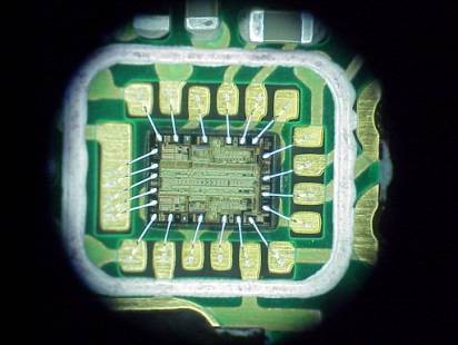
- COB: Chip-On-Board; a bare silicon chip, that is usually an integrated circuit, is supplied without a package (usually a lead frame overmolded with epoxy) and is attached, often with epoxy, directly to a circuit board. The chip is then wire bonded and protected from mechanical damage and contamination by an epoxy "glob-top".

- COF: Chip-On-Flex; a variation of COB, where a chip is mounted directly to a flex circuit.
- COG: Chip-On-Glass; a variation of COB, where a chip, typically a Liquid crystal display (LCD) controller, is mounted directly on glass:.
There are often subtle variations in package details from manufacturer to manufacturer, and even though standard designations are used, designers need to confirm dimensions when laying out printed circuit boards.
Reference
http://en.wikipedia.org/wiki/Surface-mount_technology
http://www.dl7avf.info/charts/smdcode/cs.html#TOC
สมัครสมาชิก:
บทความ (Atom)